

Top 10 Chips Production Line Innovations Revolutionizing Manufacturing
2026-05-23
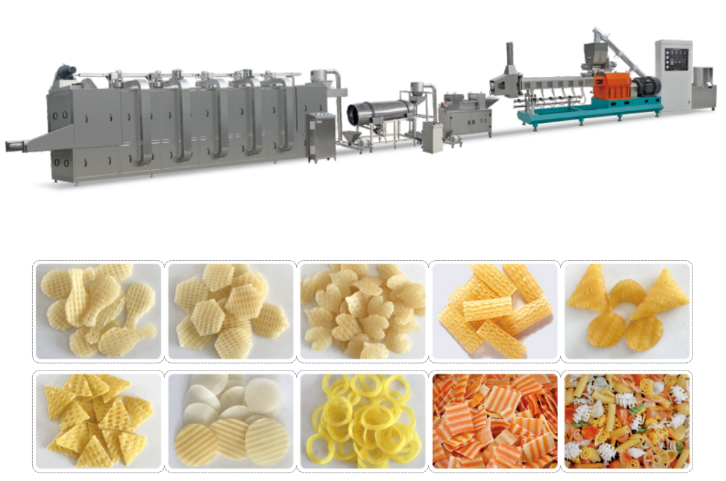
Chip production is undergoing a quiet revolution. Behind every crunchy bite lies a symphony of precision engineering, and the latest production line innovations are rewriting the rules of efficiency, quality, and scalability. At the forefront of this transformation is MINGDE, whose breakthroughs are setting new benchmarks for the industry. From intelligent frying systems to automated seasoning stations, these ten game-changing advancements aren’t just incremental upgrades—they’re reshaping how snack manufacturers think about their lines. Whether you’re scaling up output or chasing that perfect golden crisp, understanding these innovations is your first step toward staying competitive in a rapidly evolving market.
Lights-Out Factories: The Rise of Fully Autonomous Chip Manufacturing
The traditional image of a semiconductor fab is one of technicians in bunny suits hovering over gleaming tools, but a quiet revolution is under way. Lights-out factories, where production runs entirely without human presence on the floor, are no longer a futuristic concept for chip manufacturing. In these facilities, robots ferry wafer lots between automated process tools, while artificial intelligence continuously tunes recipe parameters based on real-time sensor data. The goal isn’t just to cut labor costs—it’s to eliminate contamination from human operators, reduce variability, and push yields to levels that would be impossible with manual oversight.
Achieving fully autonomous operation demands a tightly integrated stack of technologies. Advanced machine vision and edge computing allow each tool to detect microscopic defects and adjust on the fly, while predictive maintenance algorithms listen to subtle changes in pump vibrations or chamber pressure, ordering a part swap well before a failure disrupts production. The entire facility becomes a closed-loop system: material handling systems negotiate paths to avoid congestion, and a central orchestration layer reshuffles lot priorities when a tool unexpectedly goes offline. Perhaps most critically, the software architecture must handle exceptions without waking a human engineer—something that requires sophisticated cause-effect modeling and a deep library of annotated failure scenarios.
Despite the promise, full lights-out operation remains elusive for the most advanced nodes. Etch steps and lithography still encounter rare process excursions that stump even the best AI models, and the sheer complexity of high-mix production means the system must be fiercely adaptive. Yet industry leaders are inching closer every quarter, driven by the relentless scaling demands of sub-3 nanometer technologies. As these factories become more autonomous, the role of human expertise shifts from direct intervention to strategic oversight—designing the learning frameworks, curating training data, and setting higher-level objectives that the factory tirelessly works to meet.
AI-Driven Defect Detection Cuts Waste by Half
Manufacturers have long struggled with the costly balance between quality control and production speed. Traditional inspection methods, often reliant on human eyes or rigid rule-based systems, miss subtle defects or flag too many false positives, leading to unnecessary scrap. AI-driven defect detection changes this dynamic by learning from thousands of product images to spot anomalies with high precision. In one electronics assembly plant, integrating a custom vision model cut material waste by nearly half within the first quarter, simply because it caught microfractures and misalignments earlier in the line.
The real savings come from the system’s ability to distinguish between cosmetic blemishes that are harmless and functional flaws that demand immediate action. Before AI, operators might reject an entire batch for a faint surface scratch that didn’t affect performance. Now, deep learning algorithms trained on graded defect databases make consistent, split-second judgments, drastically reducing the over-rejection of usable parts. A textile mill reported that after deploying AI cameras, they diverted over 30% of previously discarded fabric back into production, cutting overall material loss by more than half.
Beyond just scrap reduction, these systems continuously adapt. When a new product variant or a different raw material batch shifts the defect profile, the model can be retrained on a small set of labeled examples without overhauling the production line. This agility prevents the kind of accumulation waste that occurs when processes drift out of spec over weeks. As a result, plants achieve a leaner operation where waste drops not as a one-time improvement but as a sustained outcome of intelligent, self-correcting inspection.
3D Packaging: Stacking Chips for Unprecedented Performance
Stacking silicon dies vertically is redefining what’s possible in semiconductor design, breaking free from the constraints of flat chip layouts. By layering memory, logic, and even analog components atop one another, 3D packaging dramatically shortens interconnect paths, slashing latency and power consumption while unlocking bandwidth that traditional 2D designs can only dream of. This isn't just about cramming more transistors into a package—it’s about architecting chips in three dimensions to handle the massive data flows of modern workloads like AI training and real-time ray tracing.
The real magic lies in the density and speed of chip-to-chip connections. Techniques like hybrid bonding and through-silicon vias (TSVs) allow thousands of vertical links per square millimeter, creating a microscopic highway system that far outpaces even the fanciest interposers. Imagine a processor that can chat with stacked memory at terabyte-per-second speeds without the energy drain of driving signals across a circuit board. That's the kind of leap 3D stacking delivers—turning what used to be distant memory calls into near-instant lookups.
Yet pulling this off demands rethinking everything from thermal management to signal integrity. Stacking chips generates intense heat in a tiny volume, forcing clever solutions like embedded microfluidic cooling and thermal-aware floorplanning. Meanwhile, designers must balance vertical communication against the physical stress of bonding ultra-thin layers without cracking. It's a high-wire act, but the payoff is a generation of processors that feel less like single chips and more like densely integrated systems, ready to power the next wave of immersive experiences and data-center breakthroughs.
Extreme Ultraviolet Lithography Breaks the Nanometer Barrier
The shift to extreme ultraviolet (EUV) light, with a wavelength of just 13.5 nanometers, has fundamentally redefined what is possible in chip fabrication. Unlike earlier deep ultraviolet systems that struggled to pattern features below 40 nanometers using complex multipatterning tricks, EUV provides a single-exposure path to critical dimensions well below 20 nanometers. This leap required rethinking nearly every subsystem: a pulsed laser vaporizing tin droplets to generate plasma, ultra-smooth multilayer mirrors that reflect light at near-grazing angles, and a vacuum environment to prevent any absorption of the delicate beam. The result is a tool capable of printing lines so fine that tens of billions of transistors can now coexist on a sliver of silicon the size of a fingernail.
EUV’s arrival also overturned long-standing assumptions about resolution limits. Engineers once believed that feature sizes below the wavelength of the light source were unreachable without exotic and costly workarounds. Yet EUV optics, combined with advanced photoresist chemistries, exploit near-field effects and photon-shot-noise management to define patterns smaller than the theoretical diffraction boundary. This sub-wavelength imaging isn’t merely an incremental improvement—it unlocks a regime where materials behave differently, and where atomic-scale roughness on a mask can make or break a chip’s functionality. In production, this means that the once-insurmountable “nanometer barrier” has been shattered, with 3nm and 2nm process nodes becoming not just feasible but commercially viable.
Perhaps the most profound consequence of EUV lithography is how it reshapes the entire semiconductor ecosystem. Design rules that were once constrained by lithographic compromises are now relaxed, allowing circuit architects to optimize for power and performance rather than printability. The technology also reduces the need for multiple patterning steps—cutting mask counts, process time, and defect risks—while enabling denser interconnects and new transistor architectures like gate-all-around designs. As the industry absorbs these changes, the focus shifts from merely breaking the nanometer barrier to harnessing EUV’s precision for the next wave of innovation: memory chips with unprecedented storage density, processors that sip power, and sensors that see the world in finer detail than ever before.
Smart Materials: Self-Healing Substrates and Beyond
The concept of materials that can mend themselves after damage once seemed like pure fantasy, but recent advances have turned it into a tangible engineering pursuit. Self-healing substrates typically rely on embedded microcapsules or vascular networks that release healing agents when cracks form, or on reversible polymer bonds that re-associate upon damage. What makes these systems compelling is not just their ability to restore mechanical integrity, but the way they blur the line between passive structure and active system. Instead of merely tolerating gradual degradation, the material itself becomes a participant in maintenance, reacting to stress without external intervention.
Beyond simple crack repair, researchers are now exploring substrates that can sense the location and severity of damage, then trigger a tailored response. Conductive fillers, shape-memory alloys, and dynamic chemical linkers are being combined to create materials that don't just heal—they adapt. In aircraft skins, for instance, a self-healing composite might restore conductivity to de-ice critical surfaces, or an architectural coating could re-seal after seismic cracking without human inspection. The shift is toward multi-functionality: the substrate becomes a platform for integrating sensing, actuation, and even energy harvesting into a single, resilient matrix.
Looking ahead, the real leap will come from programming these materials to operate autonomously over long lifecycles. Current demonstrations still often require heat, UV, or mechanical stimulus to initiate repair, but true autonomy is on the horizon with chemistries that respond directly to environmental triggers like moisture or pH changes. When combined with biodegradable or recyclable matrices, self-healing properties could dramatically cut waste in packaging, electronics, and construction. The vision is a class of materials that not only survive in harsh conditions but actively maintain themselves, ushering in a new era where 'disposable' is replaced by 'regenerative' at the substrate level.
Digital Twins Simulate Every Fab Process Before It Happens
Walking through a fabrication plant, you’ll rarely hear anyone talk about trial-and-error anymore. Instead, what’s buzzing in the background is a virtual mirror of every machine, gas line, and wafer movement. This isn’t some futuristic concept—it’s a digital twin that runs a complete dress rehearsal of the production cycle days or even weeks before the physical work begins. It catches misalignments in lithography, flags thermal drift in etching chambers, and reroutes material flow when a bottleneck shows up in the simulation. The result isn’t just avoiding scrap; it’s about turning what used to be reactive firefighting into a calm, pre-scripted sequence where surprises are engineered out before they ever touch silicon.
The real shift happens when these twins stop acting like solitary snapshots and start behaving like a living, breathing organism. Instead of modeling one tool in isolation, they stitch together an entire process chain—from wafer start to final test—and run time-lapsed simulations that factor in wear patterns on consumables, subtle shifts in chemical bath concentrations, and even the way a maintenance tech might tighten a bolt differently on any given Tuesday. One fab I visited showed me how they use the twin to shadow every lot through its journey: if a furnace tube recovery rate dips below a threshold in the virtual world, the system quietly adjusts downstream metrology recipes so no physical lot ever sees the problem. It’s not just prediction; it’s a continuous dialogue between the digital and the real, where the twin learns from every data point and reshapes the future state with each new piece of information.
What makes this feel different from classic simulation is the sheer granularity and the fact that it never sleeps. These twins are fed by torrents of sensor data—vibration spectra, gas partial pressures, RF impedance traces—and they don’t just replay the past; they generate thousands of branching “what-if” scenarios every minute. I’ve seen engineers sit in front of dashboards and watch a twin navigate a supply chain hiccup by silently shifting the order of hot lots, tweaking gas ratios, and even reordering preventive maintenance tasks—all before the morning coffee has cooled. And because the twin retains a memory of every such decision, it gets savvier over time, building an intuition that starts to mirror the gut feel veteran technicians had years ago, but backed by relentless physics-based modeling. That’s when you realize this isn’t about automation replacing human judgment—it’s about giving people a time machine to test every crazy idea without ever risking a real wafer.
FAQ
The shift to extreme ultraviolet (EUV) lithography has been a game-changer, allowing fabs to print incredibly fine features on wafers and keep Moore's Law alive despite physical limits.
Many are turning to AI-powered process control systems that monitor thousands of variables in real time, catching defects early and adjusting recipes on the fly without human intervention.
Absolutely, but it's not just about automation. Collaborative robots now work alongside technicians, handling delicate wafer transfers and tedious inspection tasks while learning from their human counterparts.
Advanced predictive maintenance, driven by sensor fusion and machine learning, is preventing unplanned downtime and minimizing scrapped batches by forecasting equipment failures days in advance.
Modular production line designs are gaining traction—they let manufacturers reconfigure tool layouts and switch between product types in hours instead of weeks, which is crucial for diverse chip portfolios.
Smart thermal management systems use digital twins to simulate and optimize cooling in real time, cutting energy consumption by double-digit percentages while keeping processes stable.
3D stacking and heterogeneous integration have moved from R&D to the production floor, letting companies combine logic, memory, and analog components in ways that boost performance without requiring smaller transistors.
Conclusion
The semiconductor manufacturing landscape is undergoing a profound transformation, driven by a suite of breakthroughs that are fundamentally reimagining the production line. Lights-out factories represent the pinnacle of this shift, leveraging advanced robotics and AI to achieve fully autonomous chip fabrication with minimal human intervention. This evolution is paired with extreme ultraviolet lithography, which has shattered the nanometer barrier, allowing for the continued miniaturization that underpins modern computing power. Meanwhile, AI-driven defect detection systems are slashing waste by more than half, using real-time analytics to spot imperfections invisible to the human eye. These technologies do not operate in isolation; they are increasingly integrated through digital twins, which simulate every fab process before it physically occurs, enabling preemptive optimization and risk mitigation.
Complementing these digital advances are breakthroughs in physical design and materials. 3D packaging stacks chips vertically, delivering unprecedented performance density without expanding the chip’s footprint, while smart materials like self-healing substrates enhance reliability and longevity. Such innovations collectively enable a new era of manufacturing intelligence where lines are not only faster and more precise but also adaptive and self-correcting. The result is a fundamental redefinition of chip production—one that promises higher yields, lower costs, and a dramatic reduction in environmental impact, cementing these advances as the cornerstones of tomorrow’s semiconductor fabrication.
Contact Us
Contact Person: LILY SUN
Email: [email protected]
Tel/WhatsApp: 0086-13969103791
Website: https://www.snackfoodmachinery.com/