

Top Wafer Cleaning Systems for Advanced Semiconductor Manufacturing
2026-10-13
In advanced semiconductor manufacturing, even a few stray particles can wreck yields. That’s why choosing the right wafer cleaning system is less about maintenance and more about competitive survival. This guide cuts through vendor hype to spotlight the top cleaning platforms actually proving themselves in high-volume fabs. You’ll also see how Siansonic is carving out a niche with precision megasonic and ultrasonic cleaning that process engineers are starting to trust.
Why Particle Removal Still Keeps Engineers Up at Night
Particle removal sounds like a solved problem until you look at the numbers on a modern logic or memory line. A single 20-nanometer particle can bridge two adjacent fins in a FinFET or bury itself at the bottom of a high-aspect-ratio trench, turning a wafer that passed every inline inspection into scrap after electrical test. The real headache is that these particles aren't just sitting on flat surfaces anymore. They're tucked under overhangs, trapped in re-entrant profiles, or electrostatically glued to low-k dielectrics that can't handle aggressive wet cleans. Every new node shrinks the critical defect size faster than the cleaning tools can adapt, so engineers spend nights balancing removal efficiency against material loss, pattern collapse, and surface roughness.
Then there's the measurement gap. In many fabs, particle inspection tools struggle to resolve defects below 40 nanometers on patterned wafers, so you can literally have killer particles that no one sees until yield drops. When a tool does flag something, the next shift has to figure out whether it came from the CMP slurry, a degraded O-ring, outgassing from the resist strip, or even a broken robot bearing. That detective work often means pulling wafers for SEM review at 3 a.m., only to find the defect has shifted or vanished during handling. Add in the fact that aggressive cleaning can create its own yield-killing residues or leave behind a monolayer of organic film that blocks subsequent deposition, and the "simple" act of particle removal becomes a high-stakes optimization problem with no universal answer.
Perhaps the most underrated reason engineers lose sleep is the industry's own success at reducing baseline defect counts. As cleanrooms get cleaner and processes more tightly controlled, the remaining particles are increasingly rare but also increasingly destructive. A single excursion event—a clogged nozzle, a transient vacuum burst, or wafers slipping in a cassette—can contaminate an entire lot within minutes. Because these events are intermittent, traditional statistical process control often fails to catch them before they hit the line, and the root cause may not repeat for weeks. So engineers keep staring at particle maps, correlating tool logs with electrical bin data, and wondering if the next lot will be the one that forces a line down event. That's why particle removal isn't just a wet bench problem; it's a round-the-clock anxiety built into the physics of making things smaller.
The Chemistry Behind Spotless Wafers Without Damaging Delicate Structures
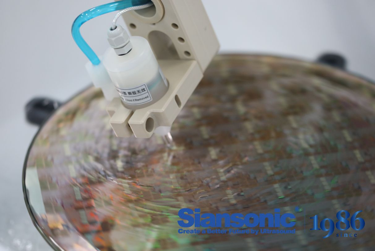
The classic SC1 bath—ammonium hydroxide, hydrogen peroxide, and DI water—removes particles by deliberately undercutting them rather than attacking the wafer. Peroxide oxidizes the silicon surface and any organic residue; ammonia then etches that thin oxide layer at a slow, predictable rate. As the oxide dissolves, particles lose their footing and float free, while high-aspect-ratio fins and 3D NAND stacks lose only a few angstroms of material.
Metal contamination calls for a different approach. Dilute hydrochloric acid turns many metal oxides and salts into soluble chlorides, but copper and silver can redeposit onto bare silicon once the bath cools or the pH shifts. Adding a chelator—citric acid, EDTA, or a phosphonate—binds those ions into stable, water-soluble complexes so they cannot plate back onto the hydrophobic surface. The redox window has to stay tight enough to avoid roughening sidewalls or leaving organic residue behind.
The final rinse can undo all of that chemistry if capillary forces pull narrow features together. Swapping water for isopropyl alcohol vapor lowers surface tension enough to prevent pattern collapse, and low-power megasonic energy can dislodge sub-100nm particles without cavitation damage. A short dilute HF step then strips any oxide grown during cleaning, leaving a hydrogen-terminated surface that sheds moisture almost instantly.
Single-Wafer vs. Batch Cleaning: Choosing Without Guesswork
Single-wafer cleaning tools offer direct control over every wafer, making them a natural fit for advanced nodes where surface sensitivity and pattern collapse are constant concerns. The ability to tune chemical flow, rinse time, and spin speed per wafer reduces variability and allows rapid recipe changes without contaminating neighboring substrates. However, that precision comes at the cost of throughput. A single-wafer tool processes one wafer at a time, which can create a bottleneck in high-volume fabs running mature technologies.
Batch immersion systems, by contrast, clean 25 to 50 wafers simultaneously in a single chemical bath, achieving much lower per-wafer cost and higher throughput for less critical layers. The trade-off is cross-contamination risk and less uniform fluid dynamics across the cassette. Choosing without guesswork means running split-lot tests on actual product wafers rather than relying on vendor benchmarks. Measure defect density, etch uniformity, chemical consumption per wafer, and cycle time under your specific film stack and cleanliness spec. Only then will the decision reflect fab economics instead of tool preference.
How Advanced Nodes Are Redefining What "Clean" Means
For years, the word "clean" in the context of network infrastructure usually meant one thing: low power draw. Data centers chased PUE ratings, and node operators bragged about kilowatts saved. But advanced nodes are quietly rewriting that definition. Today's intelligent nodes monitor their own thermal profiles, adjust processing loads in real time, and route around inefficiencies without human intervention. Clean no longer just describes energy consumption—it now covers the entire lifecycle of data handling, from how packets are validated to how heat is repurposed.
What makes this shift tangible is the way advanced nodes handle waste. Instead of treating discarded computations or redundant broadcasts as unavoidable byproducts, these nodes use predictive algorithms to trim excess before it happens. For example, a node cluster can now sense an upcoming spike in demand and spin down non-essential processes preemptively, or share cached results with neighbors to avoid repeating heavy tasks. This active reduction of digital and electrical waste goes far beyond the passive efficiency measures of the past.
The result is that "clean" has become an operational behavior rather than a static credential. A modern node isn't clean just because its hardware is efficient; it's clean because it continuously adapts to reduce its footprint while maintaining throughput. That distinction matters. It pushes the industry toward a future where cleanliness is measured not in isolated benchmarks but in the ongoing, self-correcting intelligence of the network itself.
The Overlooked Role of Drying in Yield-Critical Processes
In many yield-critical processes, drying is still treated as a straightforward moisture-removal step tucked between reaction and packaging. Yet the way a product dries can silently decide whether a batch meets specification or gets rejected. Consider an active pharmaceutical ingredient that passes every assay while wet, only to fail after drying because the crystal habit shifted under uneven heat. The loss is real, but it never shows up in the reaction yield because the chemistry was already complete. Operators often discover this only when a scale-up batch produces fines, clumps, or a polymorph that was not present in the lab.
The gap between benchtop drying and industrial drying is where many hidden yield losses live. A thin layer in a glass dish dries uniformly in minutes; a 30-centimeter cake in a tray dryer can hold a moisture gradient for hours. While the surface appears dry, the core remains wet, creating ideal conditions for hydrolysis or microbial growth. Conversely, overdrying near heating surfaces can embrittle particles, generating dust that is lost during transfer or downstream compression. These effects rarely alter the theoretical mass balance, but they change what can actually be recovered, weighed, and sold.
Teams that treat drying as a distinct unit operation with its own critical parameters tend to catch these risks before they become batch failures. Tracking drying curves, dew point, and air velocity alongside residual solvent levels can reveal a narrow window where the material is dry enough without being damaged. In one case, simply reducing the drying temperature by eight degrees eliminated a recurring 4 percent yield loss caused by agglomeration that had been blamed on the upstream crystallizer. The chemistry did not change; only the respect given to drying did.
Matching Cleaning Chemistry to New Materials Like Cobalt and Ruthenium
Bringing cobalt and ruthenium into interconnect schemes forces a rethink of wet clean formulations that were originally tuned around copper and tungsten. Cobalt does not behave like a simple drop-in replacement; it is more electrochemically active and can corrode rapidly in the presence of even mildly oxidizing species. A cleaner that worked by lightly etching copper to lift residues may create unacceptable metal loss or pitting on cobalt lines, so the oxidizer concentration, pH, and chelating package all have to be rebalanced. Ruthenium presents a different profile: its surface oxides are stubborn, yet aggressive oxidation can convert ruthenium into volatile higher oxides and erode the feature profile. Matching the chemistry to the material therefore means treating each metal as its own surface system rather than assuming a universal clean will translate.
For cobalt, the most practical formulations lean toward mildly acidic conditions with corrosion inhibitors that adsorb selectively on the metal surface. Chelators such as citric or oxalic acid derivatives can help remove post-etch residues without aggressively dissolving cobalt, but their concentration must be tightly controlled because over-chelation can still undermine the line. Galvanic coupling between cobalt and adjacent barrier layers adds another layer of complexity; a cleaner that is benign on blanket cobalt may attack cobalt when it is in contact with titanium nitride or tantalum nitride. This drives the need for electrochemical screening on patterned coupons rather than relying on blanket film etch rate data alone.
Ruthenium usually responds better to reducing or near-neutral cleaning environments that avoid extended exposure to strong oxidizers. Alkaline solutions with a mild reducing agent can lift organic residues and fluorinated polymers while leaving the ruthenium surface passivated. The key is to target the residue-to-metal selectivity, not just the residue removal rate. Screening work often combines electrochemical impedance, open-circuit potential monitoring, and cross-section SEM after patterned wafer cleans. Once a narrow window of pH, additive loading, and process time is identified, the formulation can be fine-tuned to handle both cobalt and ruthenium features on the same wafer without sacrificing either material.
FAQ
At advanced nodes, even a single sub-50 nm particle can kill a die. Cleaning steps now account for a large share of total process steps, and residue from etch, CMP, or thin-film deposition directly affects yield. The move to 3D architectures and new materials only increases the number of surfaces where defects can hide.
Most high-volume production relies on single-wafer spin cleaning for precise control, often combined with batch immersion for high-throughput steps. Dilute SC1/SC2 chemistries remain workhorses, while ozone-based processes are replacing sulfuric acid mixtures to reduce chemical use and rinse water.
Single-wafer tools offer better uniformity and lower cross-contamination risk, but batch systems still win on cost for less critical layers. Many fabs use a hybrid: batch for front-end film removal and single-wafer for pattern-sensitive cleans where damage control matters more than throughput.
Megasonic agitation creates cavitation and acoustic streaming that help dislodge particles without the mechanical scrubbing force that damages fragile features. The key is controlling frequency and power density so that cleaning effectively removes particles but does not crater narrow lines or high-aspect-ratio structures.
They are shifting to lower-energy spray techniques, dissolved-gas controlled chemistries, and cryogenic aerosol methods. Some platforms also integrate real-time surface tension management and slower rotation speeds, while advanced nozzles target only the wafer area that needs cleaning rather than flooding the entire surface.
Beyond particle removal efficiency, they should evaluate damage rate on test structures, chemical and DI water consumption per wafer, uptime with mixed recipes, and how easily the system handles backside and bevel cleaning. Compatibility with existing fab automation and the ability to switch quickly between chemistries also rank high.
Cryogenic aerosol cleaning uses solid particles of argon or carbon dioxide accelerated by a gas jet to lift contaminants through momentum transfer. It leaves no liquid residue, cuts water and chemical use drastically, and is gentle enough for delicate MEMS or high-aspect-ratio logic patterns, though its throughput is generally lower than wet strip.
As wafer starts increase and environmental regulations tighten, the cost of sulfuric acid, hydrogen peroxide, and ultrapure water becomes a major operating expense. Tools that can extend bath life, recycle rinse water, or replace hot SPM with ozone-based processes reduce both chemical spend and waste treatment load.
Conclusion
Even with years of process refinement, sub-10nm particle defects continue to erode yield because every leftover speck can short a gate or disrupt a barrier layer. Modern wafer cleaning systems lean on precisely tuned chemistries—dilute ammonia-peroxide mixtures, ozone-infused water, and specialized surfactants—that lift particles without roughening fragile fins or high-aspect-ratio trenches. Meanwhile, the choice between single-wafer and batch platforms has shifted from simple throughput math to a deeper question of defect control versus cost per wafer. Single-wafer tools deliver tighter uniformity for critical layers, while batch immersion still holds an edge for blanket films and less demanding steps. The right call often hinges on the specific film stack, not generic assumptions.
Advanced nodes have turned the definition of clean into a moving target: metal gates, low-k dielectrics, and 3D architectures tolerate far less residue and surface charge than previous generations. This pushes cleaning systems to monitor not just particle counts but also trace metals, organic films, and even moisture uniformity after rinse. Drying, long treated as an afterthought, now determines whether a wafer leaves the tool with watermark-free surfaces or a yield-killing pattern collapse. Equally critical is chemistry compatibility with emerging materials—cobalt and ruthenium interconnects corrode under traditional SC1/SC2 recipes, so new inhibitor-laced formulations and solvent-based approaches are becoming standard. Without rethinking these variables together, even the most advanced cleaning hardware falls short.
Contact Us
Contact Person: Ivy Zhang
Email: [email protected]
Tel/WhatsApp: +86 1081502288
Website: https://www.siansonic.com/